Micro-nano technologies
The development of innovative hardware components for the photonic sciences relies on advances in micro-nano technologies. Our work is therefore based on cleanroom research carried out in close collaboration with the TEAM department, and aims to overcome the obstacles to the material integration of photonic components, from materials development to the demonstration of complex multi-level processes.
III-V semiconductor technologies:
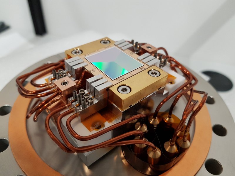
In the PHOTO team, we are carrying out in-depth work on III-V technologies and processes in GaAs and GaSb, with a view to pushing back their performance limits and combining them with other functional materials in several applications: guided optics components, vertical cavity lasers (VCSELs) (covering the spectrum from near to mid-infrared) and solar cells. What's more, our research into technological building blocks and process control solutions can be leveraged on an industrial level, as is the case with our industrial partners AET/AlOxtec and RIBER.
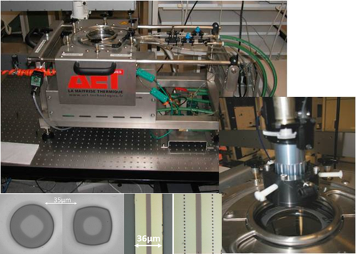
One of our specialties is the selective wet oxidation of AlGaAs alloys, a key technology for the manufacture of VCSELs and integrated optics components. Capitalizing on the previous development of a specific furnace and its real-time monitoring system, equipment that has been the subject of an industrial transfer to Grenoble-based AET technologies since 2016, our research activity currently focuses on the study of oxidation kinetics, modeling and controlling the shape of interfaces between oxide and semiconductor in 2 or even 3 dimensions, and exploiting this process to demonstrate advanced devices such as VCSELs with integrated modulators or micro-resonators with integrated access guides.
Molecular Beam Epitaxy (MBE) :
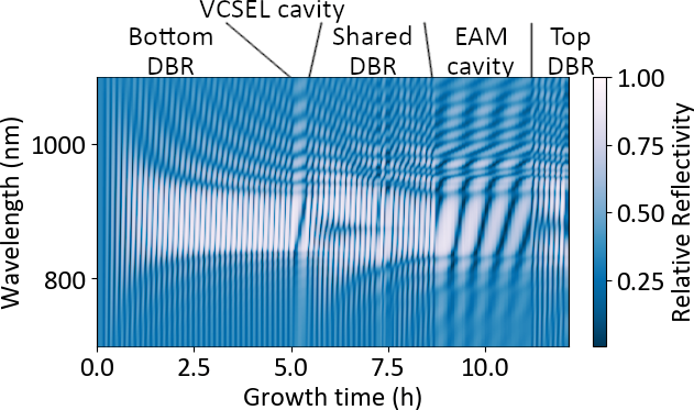
Our research is based on long-standing expertise in molecular-jet epitaxy of III-V arsenide materials. As part of a joint EPICENTRE laboratory with RIBER, we are developing new in-situ measurement tools for real-time control of the growth of complex materials and components such as VCSELs and solar cells.
Hybride technologies
At the same time, we are working to integrate new materials and components into traditional optoelectronic processes. This work covers the deposition and integration of materials using innovative processes, the development of processes for new thin-film materials such as LNOI (lithium niobate on insulator) or phase-change materials, and the hybrid integration of optical chips for complex systems.
Large area - Low cost - lithography techniques
The development of nanophotonic components requires the production of a large number of sub-micrometric, high-precision structures on a large surface area. Although e-beam lithography has been mastered by the team and the laboratory, its transposition to the scale of a whole wafer remains a challenge. We are therefore deploying technological work aimed at getting round this hurdle, based on self-assembly nanolithography techniques. (colloidal lithography, diblock-copolymers or yet soft-mold nanolithography).
Back to Photonic page