Characterization Platform
The Characterization platform brings together and organizes over 1300 m² with 150 test benches, the characterization of components and micro-nano systems in the fields: electrical, microwave, optics and biology-chemistry.
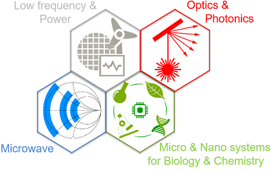
The Characterization platform hosts the characterization activity of 11 research teams and 4 start-ups with the technical support of the I2C service and under the coordination of a steering committee.
What are the four zones constituting this platform?

Electrical characterization, ESD and energy management
This area brings together the means of testing and electrical characterization of micro and nanosystems in the continuous and low frequency domain such as: I-V, C-V, impedance measurement (up to 110 MHz), parametric test, Hall effect, DLTS, thermography IR, etc. All these measurements can be carried out on bare chips using 4 stations under tips, or on encapsulated devices. Many ESD (electrostatic discharge) characterization tools are also available.
Within the ADREAM Platform, the characterization means are grouped together to qualify energy conversion systems and more particularly photovoltaic management systems. To do this, an automatic characterization bench has been specially developed in order to carry out performance tests adapted to photovoltaic requirements. The research platform has 8 test benches, allowing connection to photovoltaic modules located on the building. The benches also have connections to the electrochemical storage rooms (lead batteries, lithium, fuel cells).

Microwave characterization
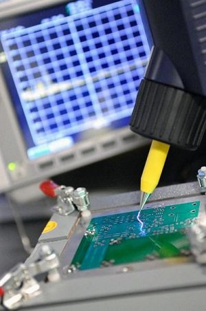
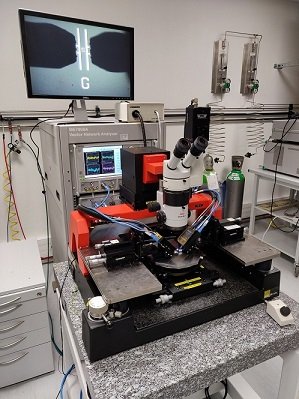
The LAAS has the means to carry out measurements of S parameters under peaks from 9 kHz up to 140 GHz. Peak spectral measurements are possible from DC up to 90 GHz. Several benches for measuring the reliability of MEMS exist (cycling, thermal behavior under RF power, etc.) including the use of a station under cryogenic tips with a controlled environment. Antenna pattern measurements are possible under peak (from 40 MHz to 65 GHz) and in an anechoic chamber (from 1 GHz to 40 GHz).

Optical Characterization
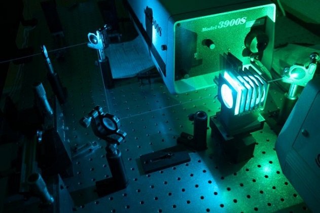
The optical characterization area brings together the experiments of researchers working in the fields of optics and photonics. These experiments range from the optical characterization of semiconductor materials to the characterizations of passive (resonant network filters, micro-cavities, etc.) and active (VCSELs, laser diodes, photodetectors, etc.) photonic components. To do this, the following means are used: PL and PLE in temperature, TFIR spectroscopy, I of V, P of I laser, divergence diagrams, spectral analysis, optical pumping of photonic crystal sources, etc. in the visible and near infrared domains.

Characterization for chemistry and biology
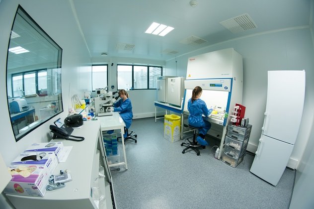
This area brings together characterization resources linked to chemistry and biology, for microelectronics. It includes two culture laboratories (cellular and microbiological), a microscopy platform, means of handling polymers and nanoparticles, electrochemistry equipment, etc. It is located in an environment suitable for the handling and storage of chemical products. In addition to these shared resources, experimentation benches closer to the research areas of certain laboratory teams: characterization of bio-NEMS, grafting of neuronal cells onto transistors, cell sorting, etc.
